Homepage von Stefan Salewski
Ein "Footprint"-Generator für PCB, das Leiterplatten-Programm der freien gEDA Kollektion
Wenn man einen Schaltplan für ein elektronisches Gerät gezeichnet hat und nun das Gerät aufbauen möchte erstellt man in der Regel eine Leiterplatte -- oft auch Platine oder "Printed Circuit Board" (PCB) genannt. Bevor die Leiterplatte physikalisch gefertigt werden kann muss ihre Struktur am Computer gezeichnet werden. Zunächst wird für jedes elektronische Bauteil ein Footprint (auch "Land Pattern" genannt) auf der Leiterplatte platziert, der u.a. passende Lötflächen und den Umriss des Bauteils vorgibt. Die Lötflächen (Pins bzw. Pads) werden dann grafisch entsprechend dem Schaltplan miteinander verbunden -- bei der Fertigung entstehen so die Leiterbahnen. Das PCB-Program der gEDA Kollektion, einer Sammlung freier Programme rund um die Elektronik (EDA) enthält bereits viele Footprints. Weitere findet man im Internet, etwa auf gedasymbols.org oder auf der Seite von John Luciani.
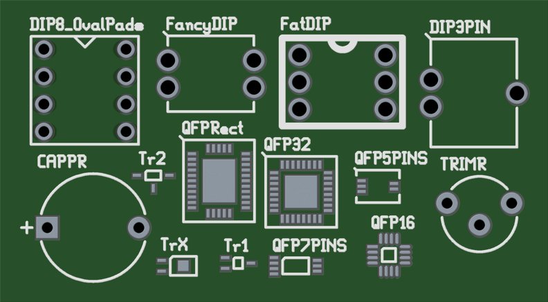
Aber manchmal fehlt eben doch einer, oder man benötigt eine ganz spezielle Variante. Also muss man den Footprint selber erstellen. Für das Programm PCB ist dies recht einfach, da die Footprints durch einfache Textdateien definiert werden, die man mit jedem beliebigen Texteditor bearbeiten kann. Für die Erzeugung neuer Footprints sind auch viele Werkzeuge verfügbar -- einige für die Kommandozeile, einige mit grafischer oder Web-basierter Benutzeroberfläche. Auf dieser Seite steht ein weiteres Exemplar zur Verfügung -- Kommandozeilen-orientiert und geschrieben in der Sprache Ruby. Hier sehen Sie einige beliebige Footprints, die für Testzwecke mit dem Programm erzeugt wurden:
Das Programm selber (Version 0.13) und einige Testdateien gibt es hier:
Das Programm wird in der Shell bzw. von der Kommandozeile aufgerufen und setzt die Existenz eines Ruby-Interpreters voraus. Starten Sie es indem Sie einfach den Namen des Skriptes in der (Linux/Unix) Shell eintippen, etwa "./sfg.rb" oder indem Sie den Ruby-Interpreter mit dem Skript als Parameter aufrufen, etwa "ruby sfg.rb". Wenn Sie das Skript ohne weiteren Parameter oder mit dem Parameter "-h" oder "--help" aufrufen wird folgender (englischer) Hilfe-Text ausgegeben:
stefan@AMD64-X2 ~/foo $ ./sfg.rb --help
sfg.rb -- yet another footprint generator for gEDA/PCB
Version: 0.12 (08-JUN-2009)
Author: S. Salewski
License: GPL

This is a plain footprint (land pattern) generator for gEDA/PCB
written in Ruby. The intention was to make its use simple, safe
and intuitive. Extension for new types of footprints is easy.

The program processes a textual input file, which contains the
parameters needed for generation of footprints. Each line of this
input file defines a single parameter, i.e. "pindiameter = 0.8 mm".

The input file is divided in sections by "Device = " statements.
You can define global parameters, if you prepend the parameters
with the line "Device = Global". Parameters specific for a special
type of footprint are defined if you prepend the parameter
definition by a command like "Device = DIP". In this case all
following parameter definitions are local. You may redefine global
parameters here, but after next "Device = " command all global
parameters have again their previous state (and no local parameters
exist). This behaviour ensures that insertion of a new section can
never influence existing sections. You can define a default unit,
so mm or mil for dimensions is optional. Equal sign for assignment
is optional too, or you may uses ":=". Numeric parameters can be
simple expressions like "2.1+0.8*2". If parameters are not numeric
and are not simple text strings, you should include it in quotation
marks. The command "Generate" followed by a filename will write the
footprint file to disk. This is a small piece of a configuration
file:

Device Global
  date "10-APR-2008"
  clearance 10 mil
  defaultunit mm

Device DIP
  defaultunit mil # locally overwrite a global parameter
  width = 300
  pins 8
  drilldiameter 0.8*1.1 mm # 10 % tolerance
  refdespos upperleft
  Generate "DIP8-300.fp" # this is a command, so do not use = sign.

If you execute this program with argument -h or --help then this
documentation is written to stdout. If you give a command line
parameter, this is considered as an input file and processing
starts. You can generate an empty input file (template) if you
give "PrintAll" as command line argument, or you may generate an
input template for a specific device by using that name, i.e.
"DIP" as argument. Redirect the output to a file and fill in the
missing information. (If you don't need the comments, then use
sed to filter the output, like "./sfg.rb List | sed s'\ #.*\\'".)

Supported device types:
-----------------------
DIP: http://en.wikipedia.org/wiki/Dual_in-line_package
SIP: Single In Line
QFP: http://en.wikipedia.org/wiki/QFP
CAPPR: Capacitor Polarized Round
TRIMR: Potentiometer or variable Capacitor, 3 pin through hole with Round outline
Dies sollte ausreichen um das Programm zu benutzen. Wenn Sie dem Programm den Parameter "List" übergeben erhalten Sie folgende Ausgabe:
stefan@AMD64-X2 ~/foo $ ./sfg.rb List
Device = Global
  author = ""
  dist-license = GPL
  use-license = unlimited
  defaultunit = "" # mm or mil
  silkwidth = 10 mil # thickness of silk lines
  silkbox = "" # inner or outer for autosize, custom for explicit size, otherwise no box
  silkboxwidth = 0 mil # silkbox width, used if silkbox = custom, no box if value too small
  silkboxheight = 0 mil # silkbox height, used if silkbox = custom, no box if value too small
  silkoffset = 10 mil # distance between pads/pins and silk lines, ignored if silkbox = custom
  textpos = upperleft # position of reference designator, upperleft, few devices accept center
  textorientation = horizontal # horizontal, some devices may accept vertical
  refdessize = 100 # size of reference designator, default is 100 (integer)
  mask = 6 mil # distance between the copper of pads/pins and the mask
  clearance = 10 mil # distance between the copper of pads/pins and any polygon
  p1silkmark = "" # mark pin/pad 1 with silk: to get a mark use: mark, p1mark, yes, true, 1
  p1coppermark = "" # mark pin/pad 1 with copper: to get a mark use: coppermark, yes, true, 1
Device = DIP
  pins =  # total number of pins
  width =  # separation of the two columns of pins -- center to center
  pitch =  # distance between adjacent pins
  pad-dia =  # outer diameter of copper annulus
  drill-dia =  # diameter of the hole
  ovalpads = "" # to get ovals use: oval, ovalpads, yes, true, 1
  p1silkmark = "" # mark pin/pad 1: global, or specific shape: semicircle, notch, damage, slash
  p1coppermark = "" # mark pin/pad 1: global section, or for specific shape: square, octagon
  # Generate ?.fp
Device = QFP
  pins =  # total number of pins
  rows = 0 # number of pins at side of pin one -- 0 is identical to pins/4
  width =  # separation of the two columns of pads -- center to center. If 0 height is used.
  height =  # separation of the two rows of pads -- center to center. If 0 width is used.
  pitch =  # distance between adjacent pads -- center to center
  padthickness =  # should be smaller than pitch
  padlength =
  ovalpads = "" # to get ovals use: oval, ovalpads, yes, true, 1
  p1silkmark = "" # mark pin/pad 1: global section, for specific shape: circle, damage, slash
  # Generate ?.fp
Leiten Sie diese Ausgabe in eine Datei um, setzen Sie die fehlenden Daten ein und verwenden Sie diese Datei dann als Eingabe für den nächsten Programmaufruf. Wenn Sie keine groben Fehler gemacht haben sollten dann Footprint-Dateien wie diese erzeugt werden:
Element["" "" "DIP8_OvalPads" "" 0 0 -19650 -27150 0 100 ""]
(
  Pin[-15000 -15000 6299 2000 7499 3937 "1" "1" ""]
  Pad[-16575 -15000 -13425 -15000 6299 2000 7499 "1" "1" "onsolder"]
  Pin[-15000 -5000 6299 2000 7499 3937 "2" "2" ""]
  Pad[-16575 -5000 -13425 -5000 6299 2000 7499 "2" "2" "onsolder"]
  Pin[-15000 5000 6299 2000 7499 3937 "3" "3" ""]
  Pad[-16575 5000 -13425 5000 6299 2000 7499 "3" "3" "onsolder"]
  Pin[-15000 15000 6299 2000 7499 3937 "4" "4" ""]
  Pad[-16575 15000 -13425 15000 6299 2000 7499 "4" "4" "onsolder"]
  Pin[15000 15000 6299 2000 7499 3937 "5" "5" ""]
  Pad[13425 15000 16575 15000 6299 2000 7499 "5" "5" "onsolder"]
  Pin[15000 5000 6299 2000 7499 3937 "6" "6" ""]
  Pad[13425 5000 16575 5000 6299 2000 7499 "6" "6" "onsolder"]
  Pin[15000 -5000 6299 2000 7499 3937 "7" "7" ""]
  Pad[13425 -5000 16575 -5000 6299 2000 7499 "7" "7" "onsolder"]
  Pin[15000 -15000 6299 2000 7499 3937 "8" "8" ""]
  Pad[13425 -15000 16575 -15000 6299 2000 7499 "8" "8" "onsolder"]
  ElementLine[-19650 -19650 -19650 19650 1000]
  ElementLine[-19650 -19650 19650 -19650 1000]
  ElementLine[19650 19650 19650 -19650 1000]
  ElementLine[19650 19650 -19650 19650 1000]
  ElementArc[0 -19650 3930 3930 0 180 1000]
  Attribute("name" "DIP8_OvalPads")
  Attribute("author" "Stefan Salewski")
  Attribute("dist-license" "GPL")
  Attribute("use-license" "unlimited")
  Attribute("date" "08-FEB-2009")
  Attribute("documentation" "www...")
)
Bitte beachten Sie, dass dieses Programm bisher nur wenig getestet wurde. Wenn Sie es verwenden, sollten Sie daher unbedingt die erzeugten Footprints sorgfältig überprüfen. Etwa indem Sie die Footprints in das PCB-Programm laden und die Abmessungen und die Nummerierung der Pins und Pads überprüfen, und indem Sie den Footprint in Originalgröße ausdrucken und die Bauteile auflegen.
Momentan unterstützt das Programm Bauteile in den Gehäusen "DIP", "SIP", "QFP" und einige andere. Es ist aber recht einfach das Programm für andere Formen zu erweitern: Erweitern Sie das Feld "datas" um die Informationen für das neue Bauteil, kopieren Sie eine der existierenden Generator-Funktionen, etwa "GenDIP()", ändern Sie deren Namen und passen Sie sie entsprechend an. Und erweitern Sie die Funktion "Generate()" um den Aufruf der neuen Funktion. Ein paar Grundkenntnisse der Sprache Ruby und des Formats der PCB Footprint-Dateien sollten dafür genügen.
Wenn Sie etwas mehr über die Sprache Ruby erfahren möchten sollten Sie sich diese (englische) Einführung ansehen:
Eine ausführliche Beschreibung des Aufbaus der PCB Footprint-Dateien gibt es von Stuart Brorson:
Oder Sie können Sich meine kurze Zusammenfassung ansehen: