Homepage von Stefan Salewski
PCB Routing
(Only english text now, sorry.)
Update -- Januar 2014
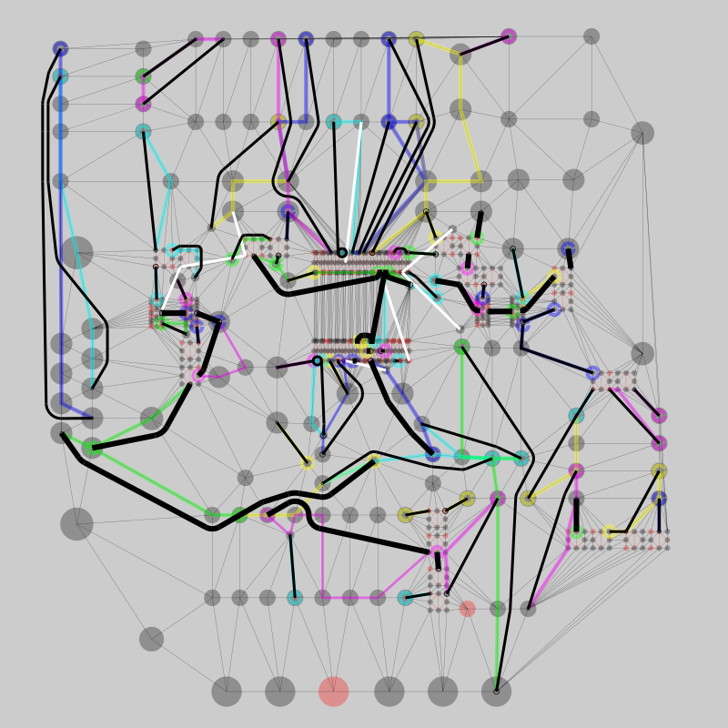
Here some recent pictures showing the current state of this router...The first two are PNG pictures of the routing result of top and bottom side of a small PCB board (tut1.pcb from current PCB program package.) Colored lines are routes of Dijkstra's shortest path search, the black curved lines are the final traces. Thin white lines indicates missing traces -- mostly a result of blocked paths. There are still some wrong wirings, i.e shortcuts or DRC violation. So there is still some work to do. I have already cleaned up the main file router.rb, so that that code is not too ugly. Cleaning up the other files is still on my todo list. The Ruby glue code for CGAL's apollonius graph is still missing on my page, so you can currently not test the router. I will try to make it available soon... The third picture is PCB's photo-mode export, only to give people not direct concerned with routing a feeling how the result may look.
For some more information please see the description below from last year.

---
In the last 18 months I spent some time investigating topological routing of printed circuit boards. Opinions about PCB routings differ very strongly between people concerned with the development of electronic circuits. Some people have the opinion that manually routings are generally of better quality. That may be true, but manually routing larger boards can take hundreds of hours. That may be OK for people enjoying that type of work or earning money with it. I myself regard it as a boring task. There are some commercial fine routers available, but in the area of free open source software the situation is not really good. Some years ago there was a very promising topological router supported by the Google summer of code project -- it was integrated in the gEDA/PCB layout tool, but it seems that the initial author has retired. The source code is available under GPL license, about 8k lines of C code. I spent some hours investigating it, but I think I am not smart enough to grab its internals.
There are some papers about topological routing freely available -- including a PhD thesis
and a master thesis. An important component of an topological PCB router is the generation
of a rubber band sketch (Other tasks are splitting nets into nets with only two terminals -- maybe by inserting steiner points,
net ordering and layer assignment). The most detailed description of this process I am aware of is contained
in the PhD thesis of Tal Dayan from 1997. (Recently I found one more PhD thesis from Mr Yan Tan about PCB routing, I have not
found time to read it yet. And there seems to be one more listed at www.ideals.illinois.edu -- about PCB routing, 17 MB file size --
but there is no free access.)
After reading Tal Dayan's thesis (not all yet), I started writing a rubber band
router. I used Ruby language, a set of randomly distributed 2D points as terminals, GTS library CGAL library
for creating the initial Delaunay triangulation. The first goal is to connect pairs of these points
with rubber band traces -- traces should not cross each other or touch other terminals. The current state,
after a few hundred hours of work, is that I have about 2000 active lines of Ruby code, which can generate the pictures
of this site.
The code is not very complicated, mostly some basic geometric operations like tangent or convex hull calculations,
Dijkstra shortest path search,
combined with the initial Delaunay triangulation from CGAL library and the important concept of regions
and region split from the above mentioned thesis. Of course the code is not really useful in its
current state -- for some randomly distributed terminals it crashes or generates invalid routings.
The crashes should be easily to fix -- it may be something like division by zero or similar exception.
The traces already behave brave -- they may touch each other or do not take the shortest path, but generally they do not cross.
Its was some fun writing the code, and I think it may be possible to extend it in the direction of a
useful router. (My initial idea was, that we should specify all the net properties, like width, clearance,
maximum allowed length, maybe impedance... prior to the routing, maybe in the schematic tool, and let the router
take care for all that. The router may even move components to reduce PCB area.)
I still have to further clean up the code, but I put it already on this page -- because I am not sure
when I will again find time and motivation to continue. To test it you will need the Ruby CGAL and BOOST library
interfaces from this page -- if you have some Ruby knowledge you will know how to use it. The command "ruby router.rb"
can be used to generate a random PNG picture.
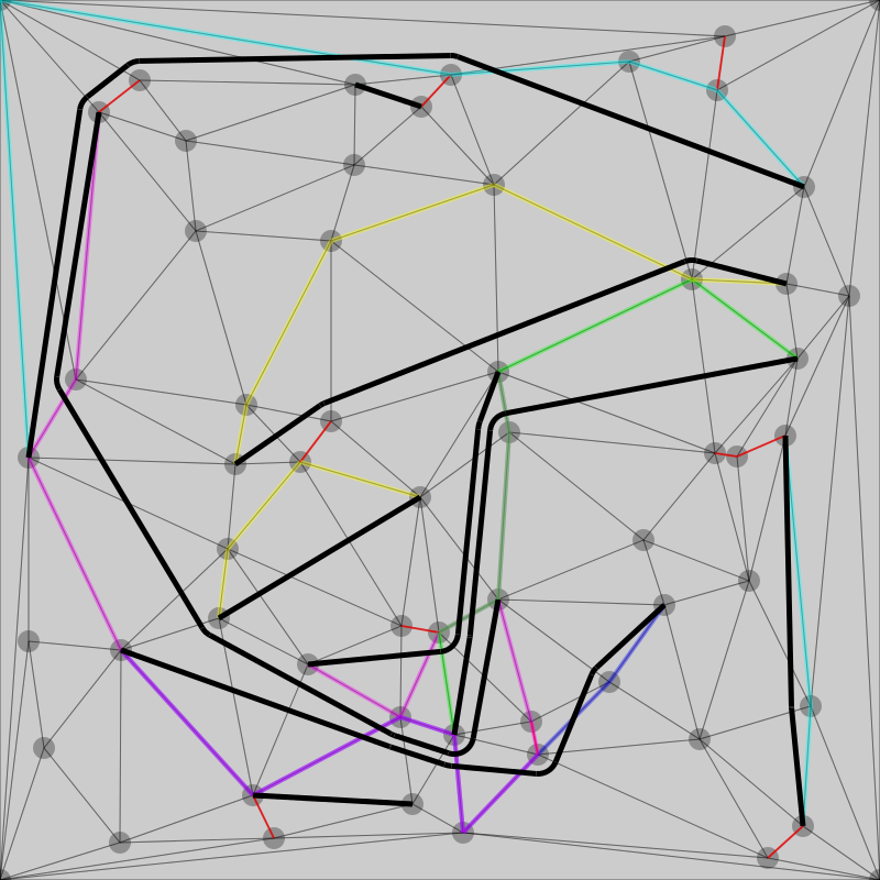
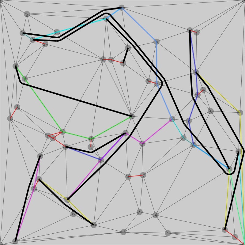
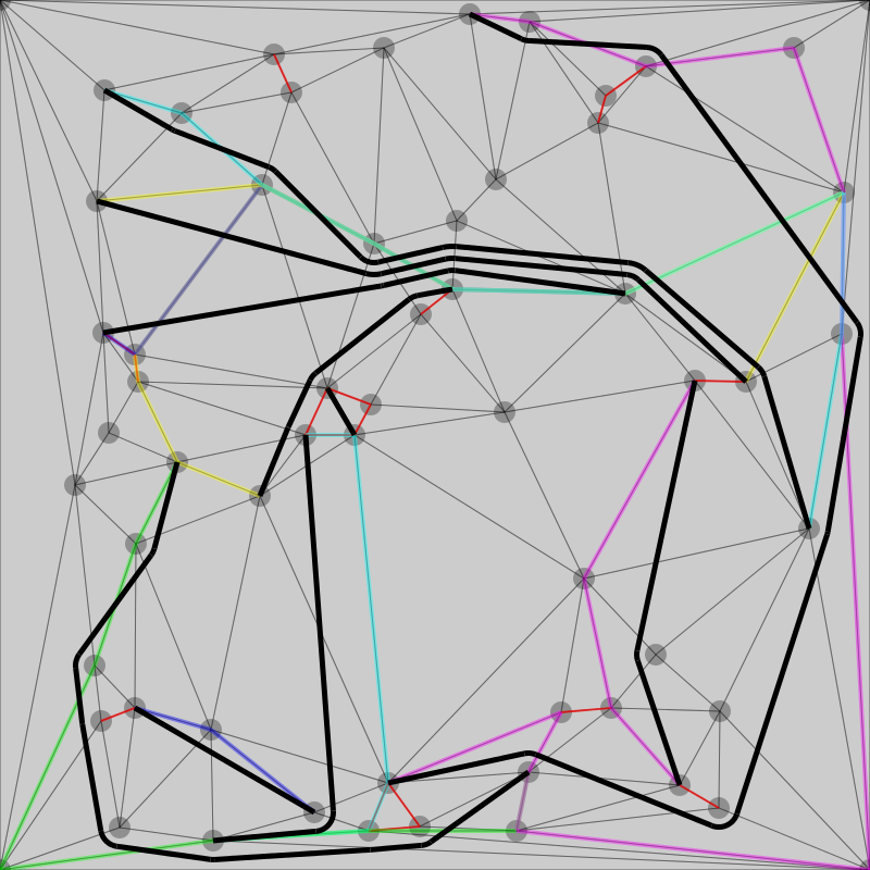
In the pictures below, the colored lines are the Dijkstra routes, the curved traces the corresponding rubber bands. Thin red lines are barriers, narrow forbidden paths. The pictures are not selected but generated randomly, so of course they contain bugs.
- Router20140107.tar
Router20131221.tarRouter20131211.tarRouter20131104.tarRouter20131026.tarRouter20131023.tarRouter20130904.tarRouter20130809.tarRouter20130706.tarRouter20130629.tarRouter20130614.tarRouter20130608.tarRouter20130604.tarRouter20130601.tarRouter20130402.tarRouter20130302.targts20121205.tar